Because an existing SoC at scale is cheaper than a custom ASIC.
You see this all the time, custom keyboard running ARM+Linux, SmartNICs using RISC-V cores/FPGAs instead of ASIC accelerators. Even Microsoft refuses to commit to ASICs for network processing in their DCs and use FPGAs instead.

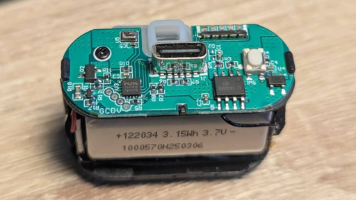
“it was actually a PY32F002B, powered by a 24 MHz Arm Cortex M0+ processor. The chip also carried 24KB of flash storage and 3KB of static RAM”
To process a single button.
that’s more powerful than my first computer
can it play Grover Teaches Typing?
Because an existing SoC at scale is cheaper than a custom ASIC.
You see this all the time, custom keyboard running ARM+Linux, SmartNICs using RISC-V cores/FPGAs instead of ASIC accelerators. Even Microsoft refuses to commit to ASICs for network processing in their DCs and use FPGAs instead.
You don’t need a CPU at all for this trash